



How does EPS filler help mitigate damage to precision circuitry during transit?
Release Time : 2026-07-23
Expanded Polystyrene (EPS) filler serves as an indispensable safeguard for precision circuitry during the complex and often hazardous transit process. The protection it provides is not merely a result of its physical bulk, but rather a sophisticated combination of customized engineering, shock absorption mechanics, and material versatility.
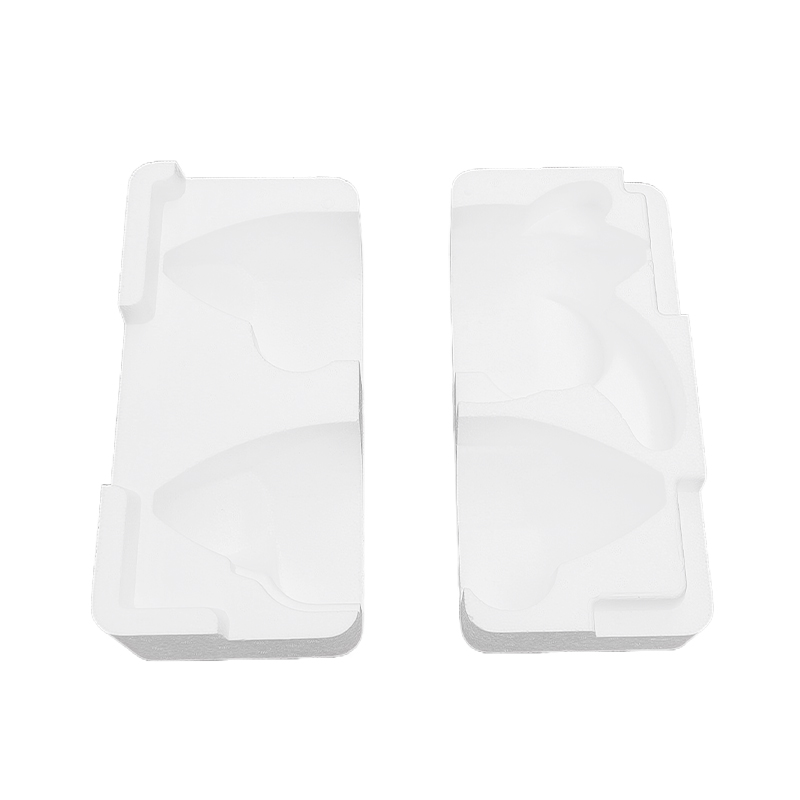
The primary defense mechanism begins with customized protection. EPS fillers are precisely designed based on the exact shape, size, and specific vulnerable areas of the electronic devices they house. Utilizing advanced molding techniques, these fillers incorporate specific grooves, protrusions, and wrap-around structures. This bespoke design ensures a tight, secure fit that completely immobilizes the precision circuitry within its packaging. By preventing any movement, the EPS filler effectively eliminates the risk of internal collision, which is a leading cause of micro-fractures in solder joints and delicate silicon wafers during transportation.
Beyond immobilization, EPS filler offers strong impact cushioning. The material's unique porous structure, composed of millions of tiny, closed air cells, acts as a highly effective shock absorber. When subjected to external forces such as bumps, drops, or sudden jolts during handling, these air cells compress and dissipate the kinetic energy. This energy absorption mitigates the direct transfer of force to the fragile components, protecting sensitive glass panels and precision circuitry from catastrophic failure.
Furthermore, the material selection for EPS fillers plays a critical role in protecting electronic components. Standard EPS can generate static electricity, which poses a severe threat to microchips. Therefore, customized EPS fillers for electronics are often engineered with anti-static properties or paired with anti-static foam and bubble sheeting. This ensures that the circuitry is protected not only from physical impacts but also from electrostatic discharge that could permanently damage sensitive pathways.
In addition to physical and electrical protection, EPS fillers also serve as a vital thermal and environmental barrier. The trapped air within the porous structure provides excellent thermal insulation, shielding precision circuitry from extreme temperature fluctuations that can occur during transit. This stability prevents thermal expansion and contraction that could otherwise compromise the integrity of the electronic assembly.
Ultimately, the mitigation of damage to precision circuitry during transit relies on a multi-layered approach. By combining precise, form-fitting immobilization with superior impact absorption and specialized material properties, EPS fillers create a secure micro-environment. This ensures that even when the outer packaging is subjected to the rigors of the supply chain, the delicate electronic heart of the product arrives safely and fully functional.
The primary defense mechanism begins with customized protection. EPS fillers are precisely designed based on the exact shape, size, and specific vulnerable areas of the electronic devices they house. Utilizing advanced molding techniques, these fillers incorporate specific grooves, protrusions, and wrap-around structures. This bespoke design ensures a tight, secure fit that completely immobilizes the precision circuitry within its packaging. By preventing any movement, the EPS filler effectively eliminates the risk of internal collision, which is a leading cause of micro-fractures in solder joints and delicate silicon wafers during transportation.
Beyond immobilization, EPS filler offers strong impact cushioning. The material's unique porous structure, composed of millions of tiny, closed air cells, acts as a highly effective shock absorber. When subjected to external forces such as bumps, drops, or sudden jolts during handling, these air cells compress and dissipate the kinetic energy. This energy absorption mitigates the direct transfer of force to the fragile components, protecting sensitive glass panels and precision circuitry from catastrophic failure.
Furthermore, the material selection for EPS fillers plays a critical role in protecting electronic components. Standard EPS can generate static electricity, which poses a severe threat to microchips. Therefore, customized EPS fillers for electronics are often engineered with anti-static properties or paired with anti-static foam and bubble sheeting. This ensures that the circuitry is protected not only from physical impacts but also from electrostatic discharge that could permanently damage sensitive pathways.
In addition to physical and electrical protection, EPS fillers also serve as a vital thermal and environmental barrier. The trapped air within the porous structure provides excellent thermal insulation, shielding precision circuitry from extreme temperature fluctuations that can occur during transit. This stability prevents thermal expansion and contraction that could otherwise compromise the integrity of the electronic assembly.
Ultimately, the mitigation of damage to precision circuitry during transit relies on a multi-layered approach. By combining precise, form-fitting immobilization with superior impact absorption and specialized material properties, EPS fillers create a secure micro-environment. This ensures that even when the outer packaging is subjected to the rigors of the supply chain, the delicate electronic heart of the product arrives safely and fully functional.